lunes, 26 de julio de 2010

Reconfigurable Patch-Slot Reflectarray Elements using RF MEMS Switches:

A microstrip reflectarray is a low-profile, inexpensive antenna which combines some of the best features of reflectors and microstrip arrays [1, 2]. Reflectarray surface which consists of isolated radiating elements is illuminated by a feed antenna. These radiating elements (patches or dipoles) are pre-designed with a particular phase delay such that the illuminating electric field from the feed will be re-radiated and scattered from these elements to form a prescribed phase front in front of the aperture. The reflectarray concept is based on the scattering properties of these radiating elements. There are several different ways to control the phase of an individual element. Some of them are - microstrip patches with the same shape and size loaded with variable length stubs [1], variable size dipoles or microstrip patches, microstrip patches with same shape but different sizes [3], identical microstrip patches on the top layer loaded with variable length slots on the ground plane [4].

The concept of reconfigurable reflectarray element is beneficial for reflectarray design as it allows for dynamic phase control of a single radiating element. Each radiating element can have a similar physical structure and the desired phase response can be achieved by electronically manipulating each element. This reconfigurable reflectarray using MEMS switches can be used as a subreflector to compensate for the distortions on the main reflector as shown in Fig. 1. This is a novel concept with future applications. The passive reflectarray can only compensate for static distortions on the main reflector while the reconfigurable reflectarray can compensate for both the static and dynamic distortions. The purpose of this paper is to investigate potential reflectarray elements by taking into consideration the eventual implementation of MEMS technology for this particular application and detailed characterization of one of the potential element designs.

Reflectarray element: Variable slot on the ground plane

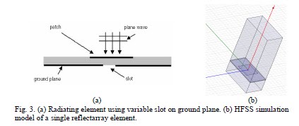
Different reflectarray designs were studied for this particular application as shown in Fig. 2. It was decided that the element with variable slot on the ground plane was best suited keeping in mind the MEMS implementation. The detailed characterization of the element involved testing the concept of reconfigurability and measurement of the phase response of a unit cell design. The principle of operation of the reconfigurable microstrip slotloaded patch reflectarray shown in Fig. 3 (a) is as follows. Radiating patch elements of equal sizes are printed on the top layer and a slot of fixed length is cut in the ground plane of each element. RF MEMS switches are implemented on the slot and length of the slot is changed by turning the switches ON/OFF. In absence of the slot, each patch radiates at its resonant frequency. The presence of slots acts as an inductive loading and introduces a phase shift. Thus, the phase of the reflected field from each unit cell of the reflectarray can be changed by determining the location of the RF MEMS switches.

Reflection Phase: Simulation and Measurement Results

Fig. 3 (b) shows the HFSS simulated model of the reflectarray element. Waveguide simulation approach was used in HFSS. Fig. 4 (a) shows the measurement setup. Figs. 4 (b) and (c) show the sample with different effective slot lengths attached to the S-band waveguide. The slot length was fixed and copper strips were used as shorting switches to reduce the effective length of the slot. The frequency (f) of operation was 2GHz (angle of incidence = 43°). The free space wavelength (λ) was 15cm and guided wavelength (λg) was 10.11mm). The unit cell size was 10.9cm x 5.5cm. Substrate with 31 mil thickness and dielectric constant of 2.2 was used. The patch size on the top layer was 4.7cm x 4.7cm (0.47 λg x 0.47 λg). The slot width on the ground plane was fixed to 0.28mm (0.028 λg). The dimensions of the copper strips (switches) were 1.5mm x 5mm. The dimensions of commercially available MEMS switches are around 1.5mm x 1.5mm. The copper strips (switches) used in the present design have the same width (1.5mm). The dimensions of the patch and the slot were chosen such that the patch is in resonance and the slot does not radiate. The only purpose of the slot is to load the patch and change the phase of the reflected field. Fig. 4 shows the comparison between the simulated and measured reflection phase results for the frequency of 2GHz. It can be seen that there is a very good agreement between the measured and simulated results. This verifies the reconfigurability concept for the design. Present efforts are on to integrate the commercially available switches in the present design and measure the reflection phase and also study the losses associated with the present geometry.

Reconfigurable feature offers electronic control of each element which provides for easier implementation of the whole reflectarray system. Several potential reflectarray element designs were investigated with critical importance given to the consideration of MEMS implementation in the final design. The reflectarray element with variable slot on ground plane and fixed patch on top was selected for final characterization. The concept of reconfigurability was tested for this design, unit cell of this reflectarray was fabricated and tested, and reflection phase measurements were performed. Future work includesmplementation of the actual switches models (MEMS) in the simulation, characterization of losses and development of an addressing scheme for the switch




Jorge Polentino
CRF
196769972


http://www.ee.ucla.edu/~harish/C9-IEEEAP-07.pdf

domingo, 25 de julio de 2010

Adaptive Antenna Array for Satellite

Antennas are classified as either single element or array antennas (multi element). Single element antennas are either omni directional or directional. Omni directional antennas have equal gain in all directions and are also known as isotropic antennas. Directional antennas have maximum gain in desired directions and less in others.

Antenna array is an arrangement of many individual antennas which are placed in space and phase such that the contribution of individual antennas add in one desired direction and cancel in other directions. The antenna arrays are used to generate electronically steer able antenna patterns. The adaptive antenna array adjusts their pattern automatically to signal environment to reduce interference. The desired signal reception is maintained by steering the main beam. Spacing between array elements is an important factor in designing antenna arrays.

Antenna array may be phased array or adaptive array. A phased array antenna system is an array of omni directional or directional element antennas in which the signal induced on the antennas are combined to form an array output. Such an antenna system controls the direction where maximum gain appears by adjusting the phase difference between different antenna elements. An adaptive antenna array combines the outputs of antenna elements but controls the directional gain of the antenna by adjusting both phase and amplitude of the signal at each individual element. Satellite antenna consists of a parabolic reflector with horn antenna at its focus. Basically horn is used as feed for parabolic reflector. Usually Horn is placed at the focus of paraboloid.. The horn antenna have desirable property that it effects a smooth transition from medium like waveguide which supports finite number of propagating modes to a medium like free space which supports a infinite number of modes.In most satellite communication systems, interference remains a problem for reliable reception of signals. Adaptive antenna array for satellite communication systems is better than omni directional antenna that radiate in all directions. Hence for this we use adaptive antenna array that automatically steer the beam in the direction of desired signal i.e. signal of interest (SOI). An antenna array has same directional performance as that of larger antenna . And radiation pattern is an important property of antenna. The overall radiation pattern of an antenna array is obtained by the radiation pattern of the individual elements, their positions, orientation in space and relative phase and amplitudes of the feeding currents to the elements.

Adaptive antenna arrays have ability to adapt changing environment conditions to maximize signal strength of signal of interest (SOI) [4]. In this paper MATLAB software has been used to obtain array voltage patterns for different values of number of elements in antenna array i.e. M and angle of beam steering i.e. x by using LMS algorithm.

ARRAY DESIGN ARCHITECTURE
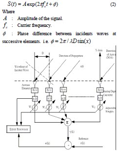
The overall array pattern can be steered in direction of desired user without physically moving any of individual elements by varying amplitude and phase of individual elements output before combining . The overall radiation pattern of an array is obtained by radiation pattern of individual elements, their positions, orientation in space and the relative amplitude and phase of feeding currents to the elements .Figure ‘1’shows adaptive antenna array whose architecture is based on LMS algorithm .It is shown in the figure that antenna array is a linear array in which centers of antenna elements are placed along straight line. Since the signals incident on all the antenna elements are of different phases due to the difference in distance traveled by the wave between two antenna elements.

The signal present at element one has traveled more distance Dsin( x) than signal present at element two [1].Where D is distance between successive antenna phase centers in the array as shown in figure 1. Therefore phase of element one will lag behind that of element two by βDsin(x).
Where

β (Phase propagation factor)= 2π /λ

Here λ =wavelength of received signal. In this figure1 the incident waves are defined as s(t) . We will assume that the receiver will down convert the signal to its Intermediate Frequency (IF) while the Analog-to-Digital converter (A/ D) will down convert the signal to its base band equivalent [4]. As they reach the antenna elements, the waves are converted to electrical sinals x(t) . From Figure1, we define the input signals as ( ), ( ),......... ( ) 1 2 x t x t x t n . These signals are then multiplied by the input weights n w ,w ,........w 1 2 . Then output signal y(t) is the weighted sum of the input signals


Where
n : Number of the weights. The error signal e(k) in the following figure represents the difference between the summed output, y(k) and the reference signal r(k) . The error processor then computes the required weight adjustment necessary in order to null out the undesired signal. This process is an iterative process and will continue until all the weights in the array converge. Consider a narrow band incident wave as:

S(t) = Aexp(2πf t +φ ) c (2)

Where
A : Amplitude of the signal.
c f : Carrier frequency.
φ : Phase difference between incidents waves at
successive elements. i.e. φ = 2π /λDsin(x)


By taking received signal at element one as the reference, the received signals x (t) i for uniform linear array with element spacing D is represented in matrix form as.


For adaptive beam forming, each element output x (t) i is multiplied with weight i w that modify phase and amplitude relation between the branches and summed to give output y(t).


The overall antenna pattern is continuously modified by adjusting weight vector. For digital communication system, the input signals are in discrete time sampled data form.

Therefore output is:

LMS ALGORITHM
Basic Description

The LMS algorithm was first introduced by Widrow et al and operates with a priori knowledge of the direction of arrival and the spectrum of the signal but with no knowledge of the noise and interference in the channel. This algorithm is useful when the interference contains some pectral correlation with the SOI. Minimization of the MMSE can be accomplished by a gradient-search technique. The particular method that the LMS algorithm uses is known as the steepest decent technique. For this particular technique, the changesin the weight vector are made along the direction of the estimated gradient vector.

Here we can see that the LMS algorithm does not require squaring, averaging or differentiating and hence can be implemented in most practical systems . Its popularity is accredited to the fact that it is simple, easy to compute and efficient. However, the drawback is that the weights for this algorithm take a long time to converge.

B. The Convergence Rate of the LMS Algorithm The parameter μ is the gain constant that regulates the speed and stability of adaptation. It determines the convergence rate. This gain factor is bounded by the limits

0 < μ <>

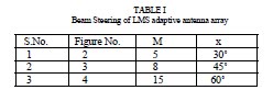
Where max λ : Largest Eigen value of the input correlation matrix. RESULTS Figures 2, 3, 4 show array voltage patterns for different values of number of elements in antenna array (M) and angle of beam steering (x) as given in table I.

The magnitude of the initial pattern is determined by the initial (arbitrary) choice of weights, w whereas the magnitude of the final pattern is determined by the strength of the desired signal, the direction and strength of the interfering signal and the noise in the system.

It is observed in figure 2, maximum gain occurs at an angle of 30° as angle of beam steering is fixed at 30°. The figure 3 shows that main beam is at an angle of 45° because signal is received by the receiver at this angle In figure 4, the maximum gain occurs at an angle of 60° as angle of beam steering is fixed at 60°


Jorge Polentino

CRF


http://www.iaeng.org/publication/IMECS2008/IMECS2008_pp1491-1494.pdf


Tipos de antenas de radar

Un phased array consiste en una matriz (array) de elementos radiantes. La fase de la señal que alimenta cada uno de estos está controlada de tal manera que la radiación del conjunto sea muy directiva. Es decir, se juega con las fases de las señales para que se cancelen en las direcciones no deseadas y se interfieran constructivamente en las direcciones de interés.

Un phased array ("agrupación de antenas controladas por fase") es un conjunto de antenas array) en el cual las fases relativas de las señales con que se alimenta cada antena se varían intencionadamente con objeto de alterar el diagrama de radiación del conjunto. Lo normal es reforzar la radiación en una dirección concreta y suprimirla en direcciones indeseadas.

Esta tecnología fue desarrollada originalmente por el futuro Premio Nobel Luis Walter Álvarez durante la Segunda Guerra Mundial, para funcionar en radares de respuesta rápida destinados a aplicaciones de Ground-Controlled Approach (GCA), es decir, de ayuda al aterrizaje de aeronaves. Más tarde se adaptó para usos en radioastronomía, valiéndole el Premio Nobel de Física a Anthony Hewish y Martin Ryle, tras desarrollar phased arrays de gran tamaño en la Universidad de Cambridge. El diseño se usa por tanto en radar y es de uso habitual en antenas de radio interferométricas.

Si todos los elementos del array están contenidos en el mismo plano y la señal con que se alimentan es de la misma fase, entonces se estará reforzando la dirección perpendicular a ese plano. Si se altera la fase relativa de las señales se podrá "mover" el haz (en realidad lo que se está haciendo es cambiar la dirección en la cual las interferencias son constructivas). Se consigue de este modo hacer barridos sin necesidad de movimiento físico, con la ventaja añadida de que se pueden escanear ángulos del orden de miles de grados por segundo. Esto permite utilizar la antena para compaginar simultáneamente funciones de detección y de seguimiento muchos blancos individuales. Apagando y encendiendo algunos de los elementos radiantes se puede variar el haz de radiación, ensanchándolo para mejorar las funciones de búsqueda o estrechándolo para hacer un seguimiento preciso de un objetivo. El punto débil de los phased arrays es la imposibilidad de dirigirlo correctamente en ángulos cercanos al plano en el que están los elementos radiantes. Para hacer una cobertura de 360º se suelen disponer 3 arrays en las paredes de una superficie piramidal.

En radioastronomía también se emplean los phased arrays para, por medio de técnicas de apertura sintética, obtener haces de radiación muy estrechos. La apertura sintética se usa tambié en radares de aviones.

El diagrama de radiación del array se obtiene como la interferencia de los campos radiados por cada una de las antenas. En recepción la señal recibida es una combinación lineal de las señales que capta cada antena. El diagrama de radiación total viene dado por el diagrama de radiación conjunto y el diagrama de radiación del elemento aislado.

En el diseño de arrays intervienen muchos parámetros : número de elementos, disposición física de los elementos, amplitud de la corriente de alimentación, fase relativa de la alimentación y tipo de antena elemental utilizada.

Configurando estos parámetros se pueden mejorar las características de radiación del diagrama de radiación individual : mejorar la directividad, mejorar la relación de lóbulo principal a secundario, conformar el diagrama para cubrir la zona de interés y tener la posibilidad de controlar electrónicamente el apuntamiento del haz principal.

El uso de los phased arrays se remonta a la Segunda Guerra Mundial, pero las limitaciones de la electrónica hacían que fueran poco precisos. Su aplicación original era la defensa anti-misiles. En la actualidad son parte imprescindible del sistema AEGIS y el sistema balístico MIM-104 Patriot. Su uso se va extendiendo debido a la fiabilidad derivada del hecho de que no tienen partes móviles. Casi todos los radares militares modernos se basan en phased arrays, relegando los sistemas basados en antenas rotatorias a aplicaciones donde el costo es un factor determinante (tráfico aéreo, meteorología,...) Su uso está también extendido en aeronaves militares debido a su capacidad de seguir múltiples objetivos. El primer avión en usar uno fue el B-1B Lancer. El primer caza, el MiG-31 ruso. El sistema radar de dicho avión está considerado como el más potente de entre todos los cazas.

En radioastronomía también se emplean los phased arrays para, por medio de técnicas de apertura sintética, obtener haces de radiación muy estrechos. La apertura sintética se usa también en radares de aviones.

Jorge Polentino

19769972

CRF


http://apa.fach.cl/temas/electr_telecom/atenas_radar.pdf

lunes, 28 de junio de 2010

Stream Memory Subsystem in Reconfigurable

Reconfigurable systems offer flexible platforms in which to optimize a memory subsystem for a single application or a class of applications. While architectural research on FPGA has been partial to processor designs, the same flexibility and performance offered by today’s FPGAs are equally suitable for the memory subsystem design. As the performance disparity between processor and memory intensifies [1], high performance or real-time application performance continues to be limited by the memory subsystem [2]. Consequently, studies on efficient memory subsystems should be considered alongside the processor design as memory performance must be scrutinized on new architectures. While FPGA platforms continue to provide a larger number of configurable logic blocks that can be mapped to processing elements to satisfy computing demands, the interconnect delays and relatively slower memories maintain an imbalance between processor and memory performance. Traditional approaches to compensate for poor memory performance such as caches are not effective due to poor temporal locality of data for streaming data [3], and especially when large memory buffers are not available on FPGA platforms. Data duplication on distributed memory buffers is also not effective as the chip area can be better utilized for processing. This paper presents a flexible memory subsystem for stream computation. The memory subsystem builds upon configurable stream units that move data while computation is performed. The stream units are specialized DMA units that are optimized for stream data transfer. They rely on a set of stream descriptors, which defines the memory access pattern, to prefetch and align data in the order required by thecomputing platform. In using the stream units in the memory subsystems, the architecture effectively decouples the communication from computation, and allows hardware designers to address their implementation and optimization ndividually. The stream units take advantage of available bandwidth by prefetching data before it is needed, and consequently, the system performance becomes dependent on average bandwidth of the memory subsystem with less sensitivity to peak latency to access a data element.
RELATED WORK
The streaming programming model separates communication from computation, allowing either programmer or compiler to specify each portion independently [4]. Properties of streaming model of computation include:
• Computations kernels are independent and self contained Computation kernels are localized such that there are no data dependencies between other kernels. A programmer can annotate portions of a program that exhibit this behavior for mapping onto a stream processor or accelerator.

• Computation groups are relatively static The processing performed in each computation group is regular or repetitive, which often come in the form of a loop structure. There are opportunities for compiler optimization to organize the computation as well as the regular access patterns to memory.

• Explicit definition of communication Computation kernels produce an output stream from one or more input streams. The stream and other scalar values which hold persistent application state are identified explicitly as variables in a communication stream or signal between kernels.

• Data movement exposed to programmer A programmer can explicitly define movement of data from memory or to other computation kernels. Hardware mechanisms such as a DMA or stream unit provide this capability without interrupting the processor. The stream processing model seeks to either minimize data movement by localizing the computation, or to overlap computation with data movement. Furthermore, the programmer can retune the application memory access as memory bottlenecks arise.


There is a number of streaming processor architectures developed over recent years. Examples of stream processors include RAW [5], Imagine [6], Merrimac [7], and the RSVP™ architecture [8,9]. There is also another class of streaming architectures with origins from reconfigurable platforms such as FPGA. These architectures rely on the flexibility of the platform to synthesize streaming accelerators based on programmer definition. In comparison to the above mentioned architectures, a set of compiler tools create optimized hardware configurations rather than map computation onto existing design. They are associated with the programming language or compiler tool that allows software developers to configure hardware for stream computation. Examples include SCORE [10], ASC [11], and Streams-C [12]. While each approach is different, stream architectures provide hardware mechanisms that can configure their datapaths for different types of parallelism in stream computation. Furthermore, they include programmable communication infrastructure to move data based on programmer defined API. In this paper, we propose the use of stream descriptors [8,9] for use in a reconfigurable FPGA platform to generate an optimized memory subsystem. Stream descriptors are a language extension to specify memory access patterns, which is used by dedicated stream units to prefetch and assemble data. The programmer describes the computation independently from stream descriptors, and then a compiler synthesizes the proper hardware for stream processing. The FPGA platform allows exploration of different configurations of the memory hierarchy. Once optimized for a particular class of applications, the design can be ported into standard or structured ASICs design flows for fabrication.


STREAM MEMORY HIERARCHY
A design framework is being developed to automatically generate synthesizable streaming accelerators [13]. Using stream programming languages [9,14,15,16] which includes programmer’s explicit definition of streams and their movement, an integrated memory subsystem can be built. This approach selects designs from well-engineered framework consisting of accelerators and network rather than generating hardware from a generic representation of a high level language [17]. The memory subsystem builds upon stream units that moves data based on stream descriptors, as shown in Figure 1. Single or multiple accelerators in various configurations can be built. Furthermore, systems with multiple scalar processors, bus, peripherals or memory controllers can be configured such that the stream unit and accelerator are placed appropriately according to the flow of data. Stream descriptors have been recently applied to stream processors [8,9] and peripherals [18,19] to leverage on the deterministic movements of data from memory. In this paper, the stream descriptors are applied to the entire memory subsystem so as to enable stream data movement throughout the computing platform. The goal of this research is to generate an optimized memory subsystem based on stream programming input. As data stream type and movement are explicitly defined, there are opportunities to optimize the memory subsystem by prefetching and overlapping movement with computation. By distributing stream units throughout the memory subsystem, the design framework avoid large cache mechanisms that are not efficient for streaming computation and are difficult to synthesize on FPGAs. This following section describes the stream descriptors used to capture stream access patterns in memory. Furthermore, an example stream unit design is described with preliminary results from synthesis.


Stream Descriptors

are mechanisms to allow theprogrammer to describe the shape and location of data inmemory. Dedicated stream units can then utilize the streamdescriptors to prefetch data from memory for the computingplatform. Each stream unit handles all issues inloading/storing of data: address calculation, byte alignmentdata ordering, and memory bus interface. A compiler can alsschedule the loading of a stream descriptor that is dependenon run time values. A stream descriptor is represented by the tuple (TypeStart_Address, Stride, Span Skip, Size) where:


• Type indicates how many bytes are in each element (Type is 0 for bytes, 1 for 16-bit half-words, etc.)

• Start_Address represents the memory address of the first stream element.
• Stride is the spacing, in number of elements, between two consecutive stream elements.
• Span is the number of elements that are gathered before applying the skip offset
• Skip is the offset is applied between groups of span elements, after the stride has been applied
• Size is the number of elements in the stream The Stride, Span, Skip, and Type fields define the shape of a data object.
The grouping and order in which data is accessed defines a Stream Record and corresponds to the preferred alignment of the computation kernel. Stream records can be processed in parallel by hardware accelerators and this explicit alignment of the data facilitates their hardware implementation by eliminating packing and unpacking instructions. Multidimensional or even non-regular spaces can be created by extending the defined semantics of each stream descriptor field. More details are available in [8,9].

Stream Unit
The stream unit consists of one or more input and output stream modules, which are generated to match the needs of the streaming accelerators. In Figure 2, there are two input and one output stream modules. The stream unit is used to transfer data from a system memory or peripheral, and present them in-order to the streaming accelerator. It also transfers processed data back to other memory locations. The following paragraph describes internal operations of the input stream module. The address generation unit (AGU) generates bus addresses based on stream descriptor values and stores pending requests in a queue (Addr Queue). The AGU has similar functionality to [20] but with more robust stream descriptors that allows for different bit-widths and more complex access patterns. The Addr Merge unit thenselects the next bus address to issue, while removing duplicate bus addresses. Data is then stored in the line buffer when the PLB bus returns data from memory. A Tag unit selects stream elements from the line buffer for storage into a stream buffer queue. Data is then presented to the streaming accelerator as aligned data, in the order defined by the stream descriptor. The output stream module consists of similar internal components, but data flows in the opposite direction. Processed data is first stored in stream buffers, which are selected for transfer by the Tag unit. A line buffer holds the set of selected stream data which can be stored at a specified bus address, stored in the Addr unit. The stream unit can be configured to match application requirements based on stream descriptor values, and characteristics of the bus-based system and streaming accelerators. For example, the number of storage elements (stream buffers) and their sizes (bit-width) are selected based on the stream descriptor values and requested bandwidth of the streaming accelerator (stream bandwidth) so that the stream module can provide the maximum number of stream elements requested per cycle. Furthermore, the Address Queue buffer size is selected based on the maximum number of pending requests supported by the bus. The bus line buffer size is set based on bus bandwidth and bursting schemes. This would allow maximum saturation of the bus that can pipeline transfer requests from the memory controller or peripherals. Finally, the address generation unit can be hardwired to generate the memory access patterns based on stream descriptors. Table 1 shows the preliminary synthesis results for different configurations of the stream unit. The resulting clock speeds is about 130MHz on the selected Xilinx FPGA device. A single configuration parameter (in columns) is varied while other parameters are held constant. In general, the larger the buffer sizes, the larger the stream unit. For larger bit-width parameter, the stream unit gate count can actually decrease due to reduced logic to handle multiple bytes within a 32bit word. The current logic circuits can be further optimized by restructuring the logic in Tag unit which compares against the bus address in Addr Queue unit when accessing the line buffer.
Jorge Polentino
19769972
CRF

Fibras De Carbono Para Hacer Displays Diminutos Y Baratos

Los ingenieros que desarrollan sistemas micro-electro-mecánicos (MEMS), quieren fabricar sus diminutas máquinas a base de silicio, porque es barato, abundante, y puede trabajarse con herramientas ya desarrolladas para fabricar circuitos microelectrónicos. Pero hay un problema: el silicio se rompe con demasiada facilidad.
Durante décadas, los investigadores han intentado fabricar pantallitas que usen diminutos espejos montados en osciladores de silicio. Pero el silicio no oscila con suficiente rapidez.

Se necesita algo sumamente rígido para oscilar con una frecuencia de resonancia de 60.000 veces por segundo (el ritmo de exploración de líneas o "actualización de pantalla" de la mayoría de los displays), pero también debe curvarse mucho para lograr el tamaño adecuado de la imagen.
Shahyaan Desai ha estado trabajando durante más de tres años en la Universidad de Cornell para crear un display práctico que encaje con los requerimientos de los MEMS.

Desai y sus colegas de la universidad, Michael Thompson (profesor de ciencia e ingeniería de los materiales) y Anil Netravali (profesor de ciencia de las fibras) han dirigido su atención hacia las fibras de carbono, el mismo material que refuerza algunas partes de automóviles, aeronaves, bicicletas, y hasta cañas de pescar.
La fibra de carbono es dos veces más rígida que el silicio, pero 10 veces más flexible.


Las fibras de carbono se fabrican de hojas delgadas y estrechas de grafito que se enrollan y upan para formar fibras. Para los usos industriales, las fibras son incluidas en los plásticos con el fin de formar materiales compuestos que son más fuertes que el acero y sin embargo más ligeros. Los MEMS de Desai están hechos con las fibras en bruto.

Desai mostró que las fibras de carbono, de dimensiones micrométricas, pueden doblarse como diminutas cañas de pescar en más de 90 grados, y pueden hacerse vibrar miles de millones de veces sin partirse. "Éste es, que sepamos, el primer material que soporta una deformación tan grande en altas frecuencias sin que aparezcan efectos notables de fatiga", explican los investigadores.

El carbono normalmente es un material quebradizo, pero en forma de fibra resiste sin romperse.

Con esta nueva tecnología, sería posible hacer un display increíblemente barato. Y el dispositivo completo sería lo bastante pequeño como para incorporarse dentro de un teléfono móvil con el fin de proyectar una imagen sobre una pared.

Además de servir como osciladores, las fibras de carbono podrían fabricarse como piezas de relojería mecánica, para impulsar una micromáquina durante un largo periodo de tiempo al liberar poco a poco su energía mecánica, o bien liberarla toda de pronto si se pretende conseguir una acción súbita de gran fuerza. También podrían emplearse como micropéndulos capaces de obtener energía a partir del movimiento, lo que haría posible alimentar teléfonos móviles, PDAs y relojes, mediante los movimientos del usuario, y logrando un nivel de eficiencia significativo.

Jorge Polentino

19769972

CRF

http://www.electronicafacil.net/archivo-noticias/ciencia/Article5415.html

MEMS: Diseño de un microrelay realizado con tecnología SOI

El desarrollo de dispositivos MEMS (Micro Electro-Mechanical Systems) ha experimentado un continuo crecimiento con nuevas áreas de aplicación. Paralelamente, la tecnología SOI (Silicon On Insulator) a demostrado ser una interesante opción para ser utilizada en la fabricación de microsensores y MEMS surgiendo en el mercado más opciones de servicios de fabricación en este tipo de tecnología. En este trabajo se presenta el diseño de un Demostrador con tecnología MEMS sobre obleas de tipo SOI para ser fabricado por la empresa Tronic's a través del sistema Europractice.
La industria de dispositivos MEMS sigue experimentando un gran crecimiento y ampliando cada vez más sus campos de aplicación. Así mismo, las exigencias del mercado hacen que crezca la demanda de dispositivos de mayor rendimiento y confiabilidad. La utilización de SOI como substrato para la fabricación de dispositivos MEMS a demostrado ser extremadamente versátil [1]. Este material tiene grandes ventajas respecto del silicio policristalino [2]. Sus principales características son el reducido “stress” residual y la posibilidad de combinar circuitos eléctricos con elementos micromecánicos. También se caracteriza por su gran resistencia en ambientes extremos y corrosivos, soportando altas temperaturas y niveles de radiación. Desde el punto de vista del diseño y la producción de MEMS, tiene además la ventaja de requerir un menor número de máscaras para el proceso de fabricación. Como consecuencia de lo expresado surgen en el mercado más alternativas para la fabricación de MEMS utilizando obleas de tipo SOI. Si a eso se le suma la posibilidad de obtener prototipos a bajo costo mediante el sistema de servicios MPW (Multi Project Wafer) la utilización de SOI para el desarrollo de MEMS se convierte en una opción viable e interesante.En este trabajo se presenta el diseño de un Demostrador con tecnología MEMS sobre obleas de tipo SOI para ser fabricado mediante el uso del servicio MPW [3], para la fabricación de prototipos, que la empresa Tronic's ofrece a través del sistema Europractice.
Diseño del demostrador
Se diseñó un Demostrador de MEMS conteniendo veintidós variantes de una unidad microrelay tomada como referencia. A partir de la estructura base del microrelay se diseñaron varios dispositivos con diferentes dimensiones y/o estructuras con el objeto de analizar su comportamiento mecánico y eléctrico. El dispositivo de referencia es un microrelay de contactos laterales accionado mediante actuadores electrostáticos de accionamiento lateral. Los actuadores están formados por dos peines, uno fijo y el otro móvil sujeto a un anclaje por medio de un resorte. El accionamiento elec-trostático presenta ciertas ventajas respecto a otros métodos alternativos. Por su parte la actuación lateral resuelve algunos de los inconvenientes que presenta el accionamiento vertical, como por ejemplo la alinealidad de la fuerza de actuación respecto al desplazamiento [4] [5]. El actuador de tipo peine provee una fuerza electrostática lineal [6] [7], producida por la aplicación de una diferencia de potencial, que depende en gran medida de las dimensiones del actuador [5]. Un parámetro importante es la tensión que se debe aplicar para producir el cierre de los contactos del microrelay. Se determinó que el aumento en el ancho de los dedos del peine, si bien logra una disminución de dicha tensión, su influencia no es muy significativa comparada con la de otros parámetros, por lo cual se mantuvo constante salvo en uno de los dispositivos solo a los fines de verificar los cálculos realizados. Los parámetros que se tomaron en consideración para el diseño de los diferentes dispositivos del Demostrador son la separación entre dedos del peine, la separación en el extremo de los dedos del peine, la cantidad de dedos y la longitud y espesor del elemento elástico. También se utilizó una estructura alternativa para éste último para evaluar su comportamiento. El tamaño del Demostrador es de 3400x3100 µm y los microrelay dentro de dicha área van desde 500x400 µm a 900x400 µm.
PROCESO SOI


El proceso de fabricación SOI utilizado [3], si bien por un lado presentó limitaciones en cuanto a la flexibilidad en el diseño, por otro lado simplificó las tareas, ya que solo fue necesario el diseño de una máscara, correspondiente a la estructura de silicio del conjunto. Las restricciones impuestas por el proceso SOI impidieron obtener la metalización de los contactos laterales del microrelay, por lo que se realizará posteriormente mediante la técnica de evaporación. Para ello se removerá el encapsulado del Demostrador colocado en la etapa final del proceso de fabricación. Se dispusieron, alrededor del área del Demostrador, una serie de pads a los cuales se conectan seis microrelay con el objetivo de ensayar algún tipo de encapsulado posterior. El tamaño de los pads es de 200x200 µm en uno de los laterales y 200x320 µm en el otro con un pitch de 240 µm en ambos casos. La capa estructural de silicio, que forma la estructura móvil de los dispositivos, es de 20 µm de espesor y la capa de óxido de la oblea SOI de 0.4 µm.


DISEÑO DEL LAYOUT


El diseño del Demostrador fue realizado en el IMEC de Leuven-Bélgica ajustándose a las reglas del proceso de fabricación. Para el diseño de la máscara se utilizó el editor de layout de Cadence, el cual está estructurado en forma jerárquica en varios niveles. El nivel más bajo lo constituyen una serie de celdas con estructuras básicas
definidas en forma paramétrica para facilitar la construcción de los diferentes dispositivos del Demostrador que difieren básicamente en sus dimensiones. Las celdas definidas corresponden a las estructuras de los peines de los actuadores, a los contactos del microrelay, a los pads de conexionado, a los anclajes de la estructura y a las vigas del resorte. La posibilidad del editor de trabajar con este tipo de celdas facilitó mucho el diseño del layout. El Demostrador diseñado se envió para su fabricación y se prevé realizar en IMEC la caracterización de los prototipos para evaluar sus resultados.


Jorge Polentino
19769972
CRF
http://www.iberchip.org/VIII/docs/posters/p27.pdf

miércoles, 23 de junio de 2010

A Capacitive RF MEMS Shunt Switch

As an example of RF MEMS devices, we propose a capacitive shunt switch for millimeter-wave application. Two types of switches have been proposed: capacitive type [6]-[12] and metal-to-metal type[12]-[15]. In general discussion as mentioned above, MEMS switches are superior in insertion loss and isolation when compared with diodes or transistors. But serious limitations such as switching speed and high driving voltage always impose some restriction on application. The reliability of mechanical actuation or mechanical contact is one of the serious concerns and must be clarified for many potential applications. Thus, MEMS switch can be applied where such advantages are essential as low insertion loss, high isolation, low signal distortion, low power consumption, etc. Capacitive switches have 'metal-to-dielectric' contact and their reliability can be higher than that of metal-to-metal ohmic contact switches. But difficulty does exist when we try to apply the capacitive switches to relatively lower frequency. As for capacitive switches, large capacitance is inevitable for resonance at relatively low-frequency range of below 10GHz, because extremely large inductance is difficult to attain with simple fabrication process. But the difficulty in the absolute value of C and L is eased when the frequency range is higher. For some application in millimeter-wave range, tuning ratio can be relatively low value of less than 10, which makes easier the actual application of capacitive switch to millimeter-wave. On the other hand, steady advance in application can be found in various fields such as automotive radar, high-speed data transfer, etc. In our previous reports [18]-[19], a prototype MEMS variable capacitor was proposed. We used the electromagnetic force to smoothly actuate the movable electrode for wide tuning range. But for reducing the size of devices, electrostatic force is preferable, as is often pointed out. In this report, we will propose a MEMS capacitive switch for millimeter-wave range which is fabricated

Basic design of capacitive switch
Figure 1 shows the schematic view of the capacitive shunt switch of single pole single throw (SPST) type. The coplanar waveguide (CPW) is along B-B’ in Fig.1(a). The movable metal electrode is on the silicon plate which is actuated by electrostatic force between he silicon plate and the electrode above the plate.


Unlike most of capacitive switches, the actuator is separated from the signal path. By separating the actuator electrode from the signal electrode, the design of electrodes can be more flexible, because the actuation electrodes do not have to meet the requirements for keeping RF characteristics. With zero actuation voltage, the movable electrode is on the CPW through insulating stopper layer (Fig.1 (b),(d)). Elastic force by silicon spring presses the


movable electrode on the CPW. RF signal is shunted to the ground because electromagnetic resonance occurs under this configuration. When the actuation voltage is applied to the actuator, the movable electrode is pulled up (Fig.1(c)). The resonance condition is no more fulfilled, and the signal goes through, which makes on-state. In this structure, movable electrode is capacitively connected to the ground. Even if the movable electrode is not resistively connected to the ground electrode, shunt switch can be realized by capacitive connection. Figure 2 shows the basic layout of electrodes and the corresponding equivalent circuit. In Fig.2(a), only the symbols for capacitors (C1,C2,C3) are drawn. The upper equivalent circuits in Fig.2(b) corresponds to the physical layout, and it can be reduced to the lower one in the figure. In order to confirm the switching behavior by the separate movable electrode, we performed three-dimensional simulation by HFSS (Ansoft corp.). Figure 3(a) shows the layout of the model for simulation and the simulated distribution of electromagnetic field is shown in Fig.3(b) for on-state and in (c) for off-state; all of the figures are for half model. The movable electrode is 60µm long along CPW (53/80/53-µm, characteristic impedance of 50Ω), and 500µm wide. The gap between the CPW and the movable electrode is set to be 3µm and 0.3µm for on- and off-states, respectively. The gap is totally air in this simulation. The input signal (76.5GHz) from the left port is clearly switched by the movable rectangular electrode. Two types of movable electrodes were employed for confirmation of the effect of matching circuits. Figure 4 shows the layout of both electrodes. As for single electrode (Fig.4(a)), movable electrode is rectangle in shape and fine meander pattern is for adjusting inductance Ls. Another is tuned one (Fig.4(b)) consisting of two electrodes and a matching circuit between them [7],[10]. The two electrodes have the same dimension with the single electrode, and they are separated by a matching circuit about 250µm long.
Structure and fabrication process
Prototype switches were fabricated by bulk micromachining technology. Figure 5 schematically shows fabrication process. (i) The glass lid with drive electrode is processed. The glass is Pyrex glass, and the electrode is Pt/Ti for this switch. A layer of SiO2 is deposited on the electrode for insulation. (ii) The cavity of about 3µm depth is formed, which defines the stroke of movable part. (iii) The glass lid and the silicon for movable part are anodically bonded with each other. Some part of metal electrode is pressed to silicon for making electrical contact for the actuator. Then the silicon is thinned to 50µm by mechanical
polishing. (iv) The movable electrode (Au/Pt/Ti) is deposited and the fixed-fixed beam is made by deep RIE. (v) The CPW electrode and stopper layer (SiO2) are formed on a silicon substrate. High-resistivity silicon (over 10Ω⋅m) is used because low-resistivity silicon deteriorate RF performance. (vi) The movable part and the CPW part are bonded with polyimide. As for sealing, polyimide may be insufficient for keeping the reliability of mechanical movement of the switch. Further research is inevitable mainly for preventing humidity. After finishing wafer process, the glass on the edge of the CPW was removed by the first dicing, and each chip was separated by final dicing. Figure 6 shows the photo of the movable part and CPW, and the bonded chip on an evaluation board. Though all the fabrication process is in wafer-level, these photos are for chips diced for specific evaluation.

RF characteristics
The S-parameters were measured by network analyzer (8510XF of Agilent Technologies) for the frequency range of 50 to 100 GHz. The switch chip was placed on the evaluation board. No electromagnetic seal was installed around the chip, and no obvious resonance due to the substrate was observed. The probes were put on the edge of CPW, and the length of CPW is 2.8mm. The driving voltage of about 50V was also applied from the pad on the CPW substrate. The insertion loss is shown in Fig.7 together with calculated result by HFSS. The measured insertion losses are 1.06dB for the single electrode and 0.77dB for the tuned electrode at 76.5GHz. At least around this frequency, the measured values agree well with calculated ones (1.19dB for single electrode and 0.68dB for tuned electrode). The loss for tuned electrode is lower than that of single electrode as


expected. As far as we know, it is quite difficult to attain the same level of performance by PIN diode or FET.

The measured isolations were 15.6dB for the single electrode and 36.8dB for the tuned electrode. The latter value of isolation is available for many applications. The measured return losses were 15.1dB for the single electrode and 23.3dB for the tuned electrode at 76.5GHz. Return loss should be controlled in many applications, and that of 20dB or better is important for them.

Discussion

The prototype MEMS switch shows a good performance for millimeter-wave range and it can be available for some applications if the conditions are ulfilled such as reliability, cost, size, etc. In designing the switch, the separate actuation mechanism can ease the restriction on the shape of electrode. If the CPW is used as actuation electrode, he size of movable electrode is determined so that the both conditions for mechanical force and RF performance can be fulfilled. So the enlargement of electrode for increasing force, for example, is not necessarily possible when RF condition is not fulfilled. For the present structure, pull-up force is partly determined by the areas of the movable silicon plate and the upper electrode on the lid, and they can be much larger than the movable electrode. The MEMS switches are superior to PIN diode or FET in insertion loss, isolation, and return loss. The equivalent circuits shows the parameters which determines the RF characteristics. When the resonance occurs, the loss is determined by the equivalent esistance Rs. The Rs is mostly determined by the esisitivity of the movable electrode, so the conductivity of the electrode metal must be high enough. By bulk micromachining, flexible condition can be employed for deposition and after-treatment, because restriction is less than surface micromachining process where movable electrode is made after the CPW is finished.
Performance improvement by the tuned electrode can be significant. As shown in Fig.4, tuned electrodes are on the same silicon plate, and they are actuated by one actuator, so only a slight increase in size is necessary for improvement by matching circuit. This s one of the advantages of the present switch. It is desirable to extend the application frequency to such lower range as 2 to 5GHz. In principle, if we can make much larger capacitance and much higher on/off atio, the structure of the present switch can be available. It is a challenge and some breakthrough will be necessary in design and fabrication process.

Monolithic integration with circuit

The above switch is fabricated by bulk-micromachining technology, which is mainly used for discrete MEMS devices. But many reports have already been made about RF MEMS devices based on surface-micromachining technology which is suitable for integration with circuit. The surface-micromachining technology utilize deposition of base materials such as polysilicon, and it is very similar to usual IC fabrication process. Obviously the monolithic integration of RF MEMS devices with circuit is very attractive. One of the most attractive advantages is to be able to use the well defined process technology. Some companies are already developing the IC for wireless communication which integrates MEMS devices. If the one-chip or System-on-Chip (SoC) solution is available, significant reduction of size and cost can be expected.
But there are many issues to overcome for achieving this kind of integration. As for process, when the MEMS devices are fabricated after finishing circuit, severe restriction is sometimes forced in order not to damage the circuit. Another issue is that the base material is limited to silicon with resistivity suitable for circuit. If high-resistivity silicon is necessary as in the above MEMS shunt switch, special processes such as epitaxial deposition is inevitable, which leads to higher cost and degrade the advantage of integration. The packaging is also an important issue for integrated MEMS devices with movable parts in it. The low-price package such as plastic mold cannot be applied and the more expensive package such as ceramic package is necessary. The area of the integrated device is larger than discrete one, so the relative cost of package can be higher if the circuit area is dominant. At present, monolithic integration is not so easy, and many approaches are made for discrete devices and researches about System-in-Package (SiP) solution is active [5]. A variety of technology for SiP have been proposed to improve the flexibility of packaging procedure.
Development of RF MEMS devices Several issues remain for the application of the RF MEMS devices. As for the devices with static displacement like switches, the following issues should be considered.

1. High driving voltage: For electrostatic actuation, relatively high voltage of around 10 to 60V is necessary for stable actuation of moving part. Though the supply current is very small, the circuit for power supply is costly. 2. Low speed: Since the mechanical displacement is necessary, operation time of less than 1µs is difficult. Typical operation time is 1 to 100µs, which limits the application of the device.

3. Relatively low reliability: The mechanical movable and the fixed parts have the possibility of sticking to each other. The mechanical strength of the movable part is generally less than that of solid devices such as diodes or transistors. So relative reliability of MEMS device is less than that of the conventional devices.

4. Packaging complexity: The package must not degrade the mechanical movement of the movable part. So the ambient material must be gas or vacuum, and corresponding package is necessary. In most cases, hermetic sealing is necessary for avoiding stiction.

5. Relatively high cost: The fabrication process is not standardized, and a variety of processes which depend on each device are inevitable. So cost reduction is more difficult than usual integrated circuits. The seriousness of the above issues depend on the device or the application. The MEMS devices show the some superior RF characteristics to that of the solid devices, but many issues must be resolved to meet the requirements for certain applications. The reliability must be guaranteed for its application, and the cost reduction is one of the most important issues. The suitable selection or creation of the application is essential for the expansion of the application.
Jorge Polentino
19769972
CRF