In this letter, a reconfigurable amplifier is designed with a tunable input and output matching network. The matching network is tuned to provide matching at different frequencies for optimum power added efficiency (PAE) and power gain. This tunability is achieved by incorporating shunt MEMS capacitive switches into the matching network. The design issues are discussed and the circuit simulation and measurement results are presented.
Active Device
The transistor used in this design is Agilent ATF-34 143 which is a high dynamic range, low noise PHEMT device packaged in a 4-lead SC-70(SOT-343) surface mount plastic package. The transistor has threshold voltage of 0.95 V and transconductance parameter of 0.24 . Based on the device arameters and the design objective, the biased condition of the transistor is chosen to be V, V and mA. This corresponds to a class AB operation. Fig. 1 shows the block diagram of the amplifier. The input matching and output matching networks provide the transistor with the optimum source and load impedances for the maximum power added efficiency and power gain. A load-pull simulation is carried out in ADS using the available device model to find out the optimum load and source impedances for the maximum power added efficiency under the particular bias condition at 8 dBm input
Reconfigurable Matching Network
It is well known that a double-stub network can provide tunable matching for different impedances. Such a matching network is composed of a fixed length transmission line and two shunt stubs. The procedure of designing a double-stub matching network is described in [7]. For a given stub spacing, d, the range of (the real part of the admittance) that can be matched is given by

 where is the imaginary part of the load impedance, is the character admittance and . The equivalent capacitance of the two stubs can then be calculated as
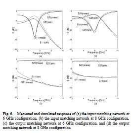
The input and output matching networks are designed following this procedure. Fig. 2 shows the schematics of the two double-stub tuner on a Si substrate. The stubs are implemented with both fixed value MIM capacitors and MEMS capacitive switches. As reported in [8], the implemented MEMS shunt switch behaves as a shunt capacitor between the center conductor of the CPW line and the ground. The capacitance of the switch can be varied to either or by activating the switch. In the input matching network [Fig. 2(a)], the second stub has capacitance of 0.65 pF (provided by MIM capacitor 2) in one configuration and 2.15 pF in the other configuration. Due to the limitation of the down capacitance that a single switch can provide, two MEMS switches are used to provide 1.5 pF when they are pulled down. In the output matching network, both stubs are implemented by one MEMS switch with down-capacitance of 0.28 pF and 0.22 pF, respectively [Fig. 2(b)]. Since the loss introduced by the MEMS switch is quite low [8], the implemented matching network has very low loss even at high frequency range.
FABRICATION PROCESS
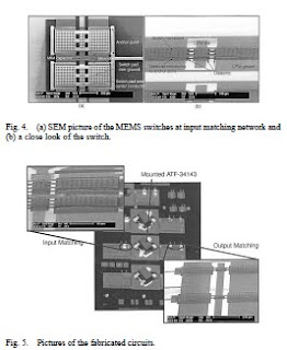
The fabrication process starts with a high resistivity Si substrate (approximately 2000 cm) covered with 2000 Si . A lift-off process is applied to define the m finite ground coplanar waveguide (FGCPW) lines, which are made of 200 of Cr and 8000 of Au. 2000 of silicon nitride is then deposited on the wafer with a PECVD process and a RIE process is followed to pattern the nitride layer.Asacrificial layer (SC1827 photoresist by Shipley) of about m is spin coated and patterned to form the anchor points for the switch and the openings for the MIM capacitor. This is followed by a sputtering deposition of m Au film. The Au film is then patterned to form the switch membrane and the top metal layer of the MIM capacitors. The process flow is illustrated in Fig. 3 and SEM pictures of the fabricated switches are shown in Fig. 4. After the circuit is fabricated, the ATF-34 143 transistor is mounted onto the wafer using conductive epoxy adhesive. Microscope pictures of the completed circuit are shown in Fig. 5.
MEASUREMENTS AND DISCUSSION


 the S-parameters of the output matching network. In the 6 GHz design configuration, the first switch is up and the second switch is down (see Fig. 2). While at the 8 GHz configuration, is down and is up. Both measured and simulated S-parameters are shown in this figure.
 The power gain and PAE of the amplifier were measured by connecting the input port to a HP 83624A Synthesized Sweeper and the output port to a HP 8564E Spectrum Analyzer. To calibrate the test setup, the circuit was replaced with a through line and the loss of the connecting cables and probes were measured. At the bias condition described in Section II and dBm of the amplifier were recorded at the two matching configurations. The power gain and PAE are calculated as
 The results are shown in Fig. 7. Simulation results are also given in the figure. The PAE and gain are improved at high frequency when the matching network is switched from configuration 1 (6 GHz design) to configuration 2 (8 GHz design). Table II summarizes the Maximum Available Gain (MAG), simulated PAE, the measured gain and PAE at two peak frequencies.
 We have demonstrated a reconfigurable amplifier design with maximum PAE and power gain at 6 GHz and 8 GHz. The adaptive matching networks are implemented with MEMS capacitive switches to provide matching conditions for both input and output at different frequencies. The RF responses of the matching networks at two design configurations are measured as well as the power performance of the amplifier.This technique can be applied to other circuit designs where reconfigurability of the circuit is required.
No hay comentarios:
Publicar un comentario